(Hong Kong)

Product Summary
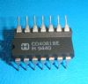
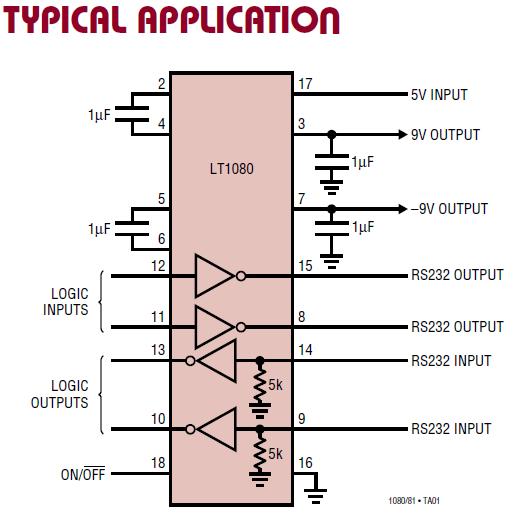
The LT1081IN is a dual RS232 driver/receiver with charge pump to guarantee absolutely no latchup. The LT1081IN provides a realistic balance between CMOS levels of power dissipation and real world requirements for ruggedness. The driver outputs of the LT1081IN are fully protected against overload and can be shorted to ±30V. Unlike CMOS, the advanced architecture of the LT1081IN does not load the signal line when shut down or when power is off. Both the receiver and RS232 outputs are put into a high impedance state. An advanced output stage allows driving higher capacitive loads at higher speeds with exceptional ruggedness against ESD. The applications of the LT1081IN include Portable Computers, Battery-Powered RS232 Systems, Power Supply Generator, Terminals and Modems.
Parametrics
LT1081IN absolute maximum ratings: (1)Supply Voltage (VCC): 6V; V+: 12V; V–: –12V; (2)Input Voltage Driver: V– to V+; Receiver: –30V to 30V; ON/OFF Pin: GND to 12V; (3)Output Voltage Driver: (V– + 30V) to (V+ – 30V); Receiver: –0.3V to (VCC + 0.3V); (4)Short-Circuit Duration V+: 30 sec; V–: 30 sec; Driver Output: Indefinite; Receiver Output: Indefinite; (5)Operating Temperature Range: –55 to 125℃; (6)Storage Temperature Range:–65 to 150℃; (7)Lead Temperature (Soldering, 10 sec): 300℃.
Features
LT1081IN features: (1)Superior to CMOS; (2)Improved Speed: Operates over 120kBaud; (3)Improved Protection: Outputs Can Be Forced to ±30V without Damage; (4)Three-State Outputs Are High Impedance When Off; (5)Only Needs 1mF Capacitors; (6)Absolutely No Latchup; (7)CMOS Comparable Low Power: 60mW; (8)Can Power Additional RS232 Drivers: 10mA; (9)Supply Current in Shutdown: 1mA; (10)Available in SO Package; (11)Available with or without Shutdown.
Diagrams
| Image | Part No | Mfg | Description |  |
Pricing (USD) |
Quantity | ||||||
|---|---|---|---|---|---|---|---|---|---|---|---|---|
 |
 LT1081IN |
|
IC DRVR/RCVR DUAL-RS232 5V 16DIP |
Data Sheet |
|
|
||||||
|
LT1081IN#PBF |
|
IC DRVR/RCVR DUAL-RS232 5V 16DIP |
Data Sheet |
|
|
||||||